Showing posts with label Company Interviews. Show all posts

Saturday, August 24, 2013

Power Electronics Technical Interview Questions [Ametek Aerospace]

Power Electronics Technical Interview Questions asked in Ametek Aerospace

               One of our friend shared his interview experience. The position is for Senior Power Electronics Engineer with 5 year experience. We believe that it will be usefull for your interview preparation...

The following questins were asked in the interview...

[1]  How to choose a micro controller?
[2]  What is the difference between a LDO and a Linear regulator?
[3]  What is the difference between I2C and SPI?
[4]  What is the difference between logic analyzer and a oscilloscope?
[5]  On what crises do we select components/Selection of a capacitor?
[6] Opamps/ADC/DAC how do you interface them externally /which ADC/DAC you have been used  and why do you selected them/resolution ?
[7]  What are usages and issues with J-Tag debugger?
[8]  Any experience in Automation?
[9]  Emi/Emc testing and how do you conduct them?
[10]  What is the ESD protection how do you select any component to be ESD protected?
[11]  Experience with other protocols Explain?
[12]  Selection of capacitor, inductor?
[13]  Frequency required and interfacing with other peripherals?
[14]  Mixed signal interfacing circuits?
[15] Emc/Emi testing for immunity and radiation testing process and how do you conduct them and  where it has been done in your product..
[16]  FMEA analysis?
[17]  Power supply design for single phase for Dc-Dc converter?
[18]  DFT,DFM Analysis,reliability,RPN number preference
[19]  Production manufacturing issues?
[20]  Design process in HW/SW?
[21]  How do you conduct design reviews?
[22]  PCB manufacturing And placement analysis?
[23] How do you come to know that a micro controller is programmable and what are the issues that occurred while debugging?

Apart from the technical questions, our friend was faced with the usual interview questions like:


 [1] Tell me about yourself?
 [2] Carrier experience and Roles?
 [3] Past and present experience?
 [4] Kind of projects handled?
 [5] Preferred area of working
 [6] Why are you looking for a change?
 [7] Willing to relocate to Bangalore?
 [8] Roles and kind of job to be handled
 About work experience and clients working for in the present organization
 Roles and reporting personalities
 Projects description.

Please share your interview experience with our readers.... 
If you like the post, then please subscribe to get new posts directly to your mail id... 
Please don't just read and go... Please leave your comments...Your comments are highly appreciated...

Saturday, November 3, 2012

TCS Campus Interview Questions Answers

These questions were asked in TCS campus interview at Govt. College of Engineering, Tirunelveli.

1. Tell me about yourself
2. About TCS
3. As a electrical engineer, why software company

4. Draw AND gate


5. what is difference between latch and flipflop

A flip-flop continuously checks its inputs and correspondingly changes its output only at times determined by clocking signal.
A latch is a device which continuously checks all its input and correspondingly changes its output, independent of the determined by clocking signal.


6. Types of flipflop:
There are basically four main types of  flip-flops: SR, D, JK, and T.


7. Do you know C
8. Are you willing to travel for onsite

...................................................................................................................................
Thanks for reading. Please leave your comments below.  Please share your interview experiences. We will post it with answers which will be useful for our readers.

Goodrich Interview: Exp.-2010

These questions are asked in the technical interview conducted in Goodrich, Bangalore for the post of Design Engineer with 2 year experience. As it is for the experienced engineers, we would have to explain as much as possible about the topic. We did not answer the non technical questions here.

A1: Question about previous exp.
A2: Question about currently working project.
[1] Explain the amplifier operation of OP-AMP?
The golden rules of OP-AMP are:
1. Vout = A. Delta Vin  [ A = Gain, Delta Vin = V+  -  V-]
2. V--  < Vout  < V++
3. Zout = 0    ,      Zin+ = Zin- = Infinity

The opamp will work as inverting amplifier and non- inverting amplifier based on the supply applied to its terminals.

Non Inverting Amplifier:
V_{\text{out}} = V_{\text{in}} \left( 1 + \frac{R_2}{R_1} \right)\,


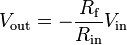
Inverting Amplifier:

V_{\text{out}} = -\frac{R_{\text{f}}}{R_{\text{in}}} V_{\text{in}}\!\,


[2]Interrupted and Asked to derive the equation...
Current i =  (Vin-Vout) / (Rin+Rf)

              =( Vin - Vx)/Rin = (Vout - Vx)/Rf

Vx = virtual ground =the node at inverting input terminal =0

[3] Interrupted and asked what is virtual ground?
Explained.
then  i = Vin/Rin - Vx/Rin = Vout/Rf- Vout/Rf

Rearranging we will get the final equation.

[4] Explain how transistor acts as a switch?
The areas of operation for a transistor switch are known as the Saturation Region and the Cut-off Region
This means then that we can ignore the operating Q-point biasing and voltage divider circuitry required for amplification, and use the transistor as a switch by driving it back and forth between its "fully-OFF" (cut-off) and "fully-ON" (saturation) regions as shown below.


Transistor Switch Operating Regions


A3: Why do you want such a high salary which is well above the market average?

......


...............................................................................................................................................
Thanks for reading. Please leave your comments below.  Please share your interview experiences. We will post it with answers which will be useful for our readers.
...............................................................................................................................................

Power Electronics Graduate Trainee Interview [BGR Energy]

These questions were asked in Power Electronics Graduate Trainee Interview conducted by BGR Energy Systems Company at MIT Chennai.

[1] Draw and Explain the SCR V-I characteristic?
Vak = +ve & Vg = 0
(i) When a positive voltage is applied to anode with respect to cathode, the junctions J1 and J3 are         forward biased, but the junction J2 is reverse biased. 

(ii) The SCR is in its forward blocking state. At this time the Gate signal is not applied. 

(iii) As shown in figure a small amount of forward leakage current is flows through the device.

Vak = + & Vg = +ve
(i) When the small amount of positive voltage is applied, while positive voltage is applied to anode with respect to cathode, the junction J3 becomes forward biased. 

(ii) Thus the SCR conducts a large value of forward current with small voltage drop. With the application of gate signal the SCR changed from forward blocking state to forward conducting state. It is called as latching.Without gate signal it happens at forward breakdown voltage (Vfbd).

(iii) When the gate signal value is increased, the latching happens for low Vak voltages as mentioned in the figure. In the presence of forward current (i.e. after the thyristor is turned on by a suitable gate voltage) it will not turn off even after the gate voltage has been removed.  

(iv) The thyristor will only turn off when the forward current drops below holding current. The holding current is defined as the minimum current required to hold the SCR in the forward conduction state.

Vak = -ve
(i) When a negative voltage is applied to anode with respect to cathode, the junctions J1 and J3 are reversed biased, but the junction J2 is forward biased. The SCR is in its reverse blocking state. 

(ii) As shown in figure a small amount of reverse leakage current flows through the device. 
If the applied voltage is more than reverse breakdown voltage, the device will collapse and the large amount of current flows through it.

[2] Explain Buck topology
(i) When the switch is ON condition (ie, TON), the input provides energy to inductor and output. 
(ii) The difference between the input and output voltage is applied to inductor as shown in the below waveform.
(iii) When the switch is turned off, the inductor current will flow in the same direction to load. It is inductor property to maintain the current flow in the same direction.
(iv) The freewheeling diode D1 is forward biased at this time and completes the inductor current path.

The output of the buck converter with continuous output current is 

Vout = D*VIN

D = Duty cycle = TON / [TON + TOFF]

[3] Compare MOSFET and BJT
             BJT                                                                     MOSFET
More Power handling Capability                             Less Power handling capability
Low switching speed                                             Fast switching speed
High On state resistance                                        Low on state resistance
Has second breakdown voltage problem                 No second breakdown voltage problem